- 您现在的位置:买卖IC网 > Sheet目录370 > ZXLD1374EST20TC (Diodes Inc)IC LED DVR BUCK BOOST 20TSSOP
�� �
�
�A� Product� Line� of�
�Diodes� Incorporated�
�ZXLD1374�
�Application� Information� (cont.)�
�Reduced� Input� Voltage� Operation�
�To� facilitate� operation� in� applications� that� have� large� transient� reductions� in� system� supply� voltage,� the� ZXLD1374� is� capable� of� operating� down�
�to� input� voltages� as� low� as� 6.3V.� Care� must� be� taken� when� operating� at� these� lower� supply� voltages� to� ensure� that� the� internal� MOSFET� is�
�correctly� enhanced� and� that� the� boosting� ratio� is� not� increased� to� excessive� amounts� where� both� the� duty� cycle� and� peak-switch� current� limits�
�are� not� exceeded.� The� device� will� operate� down� to� 6.3V,� but� for� reliable� start� up� V� IN� must� be� higher� than� 6.5V� plus� any� margins� for� any� noise�
�that� may� occur� on� the� supply� lines.�
�In� Buck-boost� and� Boost� modes� (most� common� topologies� for� applications� likely� to� require� transient� operation� down� to� supply� voltages�
�approaching� 6V)� as� the� input� voltage� reduces� then� the� peak� switch� current� will� increase� the� ZXLD1374� compensates� for� this� by� allowing� the�
�sense� voltage� to� increase� while� maintaining� regulation� of� the� LED� current.� However� if� the� boost� ratio� (switch� output� voltage/input� voltage)� is�
�increased� too� much� then� the� sense� voltage� could� be� increased� too� much� causing� an� over-current� flag� to� be� triggered� and/or� loss� of� regulation.�
�In� addition� to� this,� increased� power� dissipation� will� occur� in� the� internal� MOSFET� switch.� One� way� of� overcoming� this� is� to� apply� a� boot-strap�
�network� to� the� V� AUX� pin� –� see� next� section.�
�If� the� ZXLD1374� is� used� in� buck� mode� at� low� voltages� then� the� boot-strap� network� cannot� be� implemented� and� some� loss� of� regulation� may�
�occur� at� input� voltages� approaching� 6V� driving� 1� LED.�
�When� using� the� ZXLD1374� in� applications� with� transient� input� voltage� excursions� we� recommend� using� the� web� calculator� to� optimize� operation�
�over� the� normal� operating� band.� Then� change� the� input� range� to� include� the� transient� excursion� while� keeping� the� optimized� component�
�selection� to� check� expected� function� during� the� transient� input� voltage� conditions.�
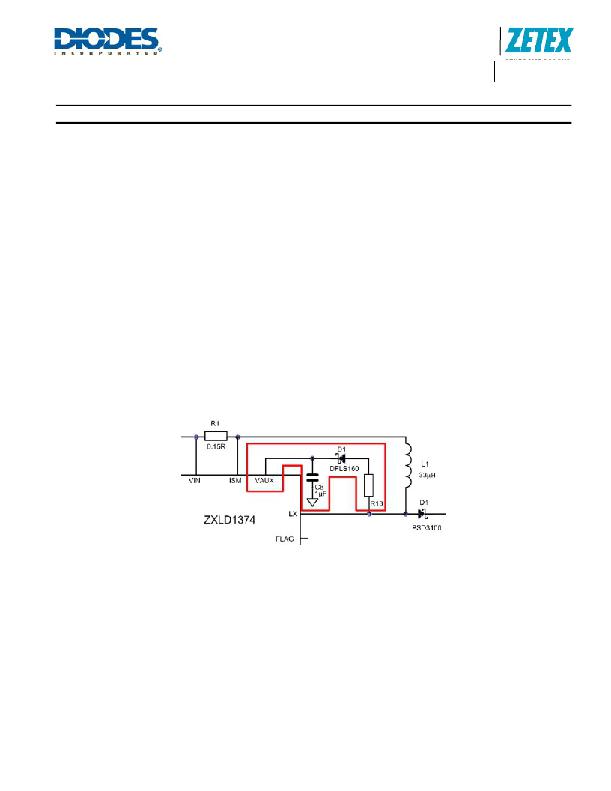
�Boosting� V� AUX� Supply� Voltage� in� Boost� and� Buck-Boost� Mode�
�A� boot-strap� boosting� technique� can� be� used� to� increase� the� gate� drive� voltage� at� low� input� voltage.� See� figure� 34� for� circuit� diagram.� This� can�
�be� particularly� important� for� extended� use� at� low� input� voltages� as� this� is� when� the� switch� current� will� be� at� its� greatest� –� resulting� in� greatest�
�heat� generation� within� the� MOSFET.�
�Figure� 34.� Bootstrap� Circuit� for� Boost� and� Buck-Boost� Low� Voltage� Operations�
�The� Bootstrap� circuit� guarantees� that� the� MOSFET� is� fully� enhanced� reducing� both� the� power� dissipation� and� the� risk� of� thermal� runaway� of� the�
�MOSFET� itself.� The� bootstrap� circuit� consists� of� an� extra� diode� D2� and� decoupling� capacitor� C8� which� are� used� to� generate� a� boosted� voltage�
�at� V� AUX� .� This� enables� the� device� to� operate� with� full� output� current� when� V� IN� is� at� the� minimum� value� of� 6.3V.� The� resistor� R13� can� be� used� to�
�limit� the� current� in� the� bootstrap� circuit� in� order� to� reduce� the� impact� of� the� circuit� itself� on� the� LED� accuracy.� A� typical� value� would� be� 100� ohms.�
�The� impact� on� the� LED� current� is� usually� a� decrease� of� maximum� 5%� compared� to� the� nominal� current� value� set� by� the� sense� resistor.�
�The� Zener� diode� may� be� used� to� limit� the� voltage� on� the� V� AUX� pin� to� less� than� 60V.�
�Due� to� the� increased� number� of� components� and� the� loss� of� current� accuracy,� the� bootstrap� circuit� is� recommended� only� when� the� system� has� to�
�operate� continuously� in� conditions� of� low� input� voltage� (between� 6.3� and� 8V)� and� high� load� current.�
�If� lower� transient� voltages� are� expected� then� the� ZXLD1371� LED� Driver-controller� could� be� used,� whose� input� voltage� extends� down� to� 5V.�
�ZXLD1374�
�Document� number:� DS35032� Rev.� 3� -� 2�
�27� of� 39�
�www.diodes.com�
�September� 2012�
�?� Diodes� Incorporated�
�发布紧急采购,3分钟左右您将得到回复。
相关PDF资料
ZXLD1937ET5TA
IC LED DRIVR WHITE BCKLGT TSOT-5
ZXLD381FHTA
IC LED DRIVR WHITE BCKLT SOT23-3
ZXLD383ET5TA
IC LED DRIVR WHITE BCKLGT TSOT-5
ZXSC300E5TA
IC LED DRVR WHITE BCKLGT SOT23-5
ZXSC380FHTA
IC LED DRVR WHITE BCKLGT SOT23-3
ZXSC400E6TA
IC LED DRVR WHITE BCKLGT SOT23-6
0-1005447-1
SENSOR PIEZO FILM VIBRA MASS
0035.1272
HOLDER LED SRL 5MM YELLOW
相关代理商/技术参数
ZXLD1601
制造商:ZETEX 制造商全称:ZETEX 功能描述:ADJUSTABLE DC - DC BOOST CONVERTER WITH INTERNAL SWITCH IN SC70
ZXLD1601H6
制造商:Diodes Incorporated 功能描述:LCD/OLED BIAS BOOST CONVERTER SMD
ZXLD1601H6TA
功能描述:开关变换器、稳压器与控制器 Boost Converter for LCD and OLED BIAS RoHS:否 制造商:Texas Instruments 输出电压:1.2 V to 10 V 输出电流:300 mA 输出功率: 输入电压:3 V to 17 V 开关频率:1 MHz 工作温度范围: 安装风格:SMD/SMT 封装 / 箱体:WSON-8 封装:Reel
ZXLD1601H6TC
功能描述:开关变换器、稳压器与控制器 Boost Converter for LCD and OLED BIAS RoHS:否 制造商:Texas Instruments 输出电压:1.2 V to 10 V 输出电流:300 mA 输出功率: 输入电压:3 V to 17 V 开关频率:1 MHz 工作温度范围: 安装风格:SMD/SMT 封装 / 箱体:WSON-8 封装:Reel
ZXLD1615
制造商:DIODES 制造商全称:Diodes Incorporated 功能描述:ADJUSTABLE DC-DC BOOST CONVERTER WITH INTERNAL SWITCH IN
ZXLD1615ET5
制造商:Diodes Incorporated 功能描述:LCD/OLED BIAS BOOST CONVERTER SMD 制造商:Diodes Incorporated 功能描述:LCD/OLED BIAS BOOST CONVERTER, SMD 制造商:Diodes Incorporated 功能描述:LCD/OLED BIAS BOOST CONVERTER, SMD; Primary Input Voltage:5.5V; No. of Outputs:1; Output Voltage:28V; Output Current:10mA; Voltage Regulator Case Style:TSOT-23; No. of Pins:5; Operating Temperature Min:-40C; Operating Temperature ;RoHS Compliant: Yes
ZXLD1615ET5TA
功能描述:开关变换器、稳压器与控制器 Boost Converter for LCD and OLED BIAS RoHS:否 制造商:Texas Instruments 输出电压:1.2 V to 10 V 输出电流:300 mA 输出功率: 输入电压:3 V to 17 V 开关频率:1 MHz 工作温度范围: 安装风格:SMD/SMT 封装 / 箱体:WSON-8 封装:Reel
ZXLD1615ET5TC
功能描述:开关变换器、稳压器与控制器 Boost Converter for LCD and OLED BIAS RoHS:否 制造商:Texas Instruments 输出电压:1.2 V to 10 V 输出电流:300 mA 输出功率: 输入电压:3 V to 17 V 开关频率:1 MHz 工作温度范围: 安装风格:SMD/SMT 封装 / 箱体:WSON-8 封装:Reel